
With the transition of electronics communication modules to higher frequencies and smaller form factors, electromagnetic interference (EMI) is now a significant issue that threatens the performance of the system. The 5G mmWave systems, aerospace avionics, and unwanted EMI in high-tech radars can adversely impact signal integrity, which can give rise to cross-talk and cause the system failure altogether. Shielding is necessary so as to make sure that there is regulation and operation. Linkworld has over 20 years of RF experience and we know that the shielding in the modern times is multilayered. This guide talks about 4 basic strategies of EMI reduction in modules of microwave communication.
Advanced Connector Shielding and Filtered Interfaces
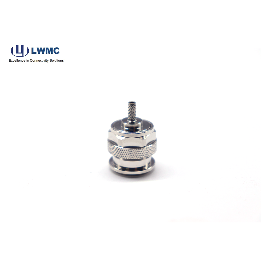
The connector interface is a very important entry port of electromagnetic energy. The continuity of ground contact 360-degree constructions provides an entirely shielded design to unwanted antennas. The I-PEX MHF® 7S series utilizes ZenShield® architecture reducing EMI of 5G mmWave devices up to frequencies of 15 GHz by terminating signal pins on stripline in receptacle ground contacts, and controlled hollow 5G mmWave impedance environments in which electromagnetic fields can be confined. In addition to this, filtered RF connectors incorporate built-in EMI suppress. The EMI is grounded by mounting stress-isolated chip capacitors between shield and mounting panel in the BNC filtered connectors of Amphenol, so as to conduct desired signal without loss. Linkworld provides customized variants of a certain EMI issue in their portfolio.
Gap Waveguide Packaging for Module-Level Shielding
Traditional shielding techniques may suffer cavity and parallel-plate propagation to couple circuits together. The gap waveguide technology is a radical solution. It is a technique in which periodic structures, either of the form of beds of nails, or lids of pins, are applied to put cutoff conditions on all parallel-plate modes of all assemblies globally (oversized). The structure is used to suppress unwanted cavity modes, substrate and EMI feedback in these stop-bands that otherwise would degrade the performance. Gap waveguide packaging Studies have shown that gap waveguide package may be applied in order to increase the isolation of microstrip circuit elements in high-frequency modules. The periodic structures are built onto module housings or lids and do not need complex internal fine tuning which offers far greater electromagnetic compatibility to space-starved applications. Linkworld's engineering team incorporates these advanced packaging techniques to deliver optimal shielding performance.
Board-Level Shielding and Absorber Materials
At the board level, conductive shields which are coupled with electromagnetic absorber materials are quite effective in suppressing EMI at PCB level. Board level shields offer shields in form of conductive barriers of the emissions and the unwanted electromagnetic energy is converted into heat by the absorber materials. The new solutions bring a combination of a number of technologies in terms of frequency bands-reflectless barriers are built with conductive gaskets and pre-shaped shields, and the energies that will otherwise be reflected at another place are absorbed by hybrid absorber materials (combination of metal and polymer). This dual strategy is effective particularly in thick boards. The attenuation of the shielding is largely dependent on the choice of material with lightweight silver/polyamide mesh having attenuation of 50 dB to 70 dB, copper/nickel/polyester composite attaining 70 dB to 100 dB with specialized copper/polyester. Where conventional techniques fail to provide the necessary margin, absorber-enhanced shielding provides the needed margin in microwave modules. These new high-tech materials are applied in the custom assemblies of the EMI-sensitive applications by the Linkworld.
Frequency-Selective Surfaces for Targeted Interference Control
Where frequency selective surfaces (FSS) may be employed in the event of interference by given frequency bands, the preferred frequencies may be passed and the unwanted frequencies rejected. These periodic structures are also referred to as spatial filters and filter out energies of specific frequencies. It is recently discovered that FSS structures are cure-all, fixing catastrophic EMI challenges such as aviation radio-altimeter (4.2-4.4 GHz) immunity to 5G sub-6 GHz (3.7-3.98 GHz) interference. The proposal makes use of suggestions that use dual-band FSS unit cells that form narrow passbands at 4.3 GHz (0.5 dB of insertion loss) and stopbands at the interfering frequencies. The structures of this kind can be placed under the antennas, and they do not demand any changes to the equipment. Radomes, housings or ground planes in modules that are operated in congested spectrum conditions are fitted with FSS to provide frequency selective protection in the absence of broadband attenuation taking into account desired signal frequencies. Linkworld evaluates FSS solutions for specific EMI issues.
Multi-layered techniques that address all the potential interference paths are the only effective way of reducing EMI. Preservation of signal integrity involves fine connectors having filtering, gap packaging consisting of waveguide, absorber based board-level shields, frequency selective surfaces. Complete shielding plans are more important within the growing frequencies and densities. Linkworld provides 20 years of RF and vast EMI control through providing components, custom assemblies, as well as engineering guidance to its clients as a way of providing high reliability where necessary in challenging applications. Get in touch with us and discuss your needs for microwave module shielding.